Extrinsic Semiconductor
An extrinsic semiconductor is a semiconductor material that has been intentionally modified by adding a small amount of another element to a pure or intrinsic semiconductor, like silicon and germanium. The additional element is known as a dopant or impurity, and the process of adding a dopant to an intrinsic semiconductor is known as doping.
Adding a dopant increases electrical conductivity. The choice of dopant is a critical factor in semiconductor manufacturing, influencing the performance and applications of electronic devices.
Types of Extrinsic Semiconductor
Different dopants have distinct effects on the semiconductor’s conductivity and behavior, giving rise to two primary types of extrinsic semiconductors: N-type and P-type.
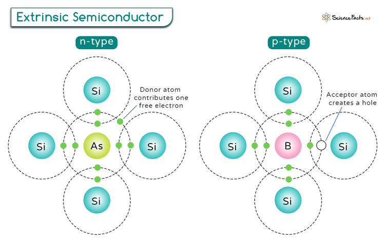
1. N-type
An N-type semiconductor is created by adding impurity atoms that have more electrons than the semiconductor material itself. Group V elements such as phosphorus (P), arsenic (As), and antimony (Sb) have five valence electrons (pentavalent) and are commonly used as dopants.
When these pentavalent impurities replace some of the host semiconductor atoms, they introduce an extra electron into the crystal structure. These additional electrons contribute to the semiconductor’s conductivity, making it more efficient in carrying an electric current.
2. P-type
A N-type semiconductor is created by adding impurity atoms with fewer electrons than the semiconductor material. Group III elements, such as boron (B), aluminum (Al), and gallium (Ga) with three valence electrons (trivalent), are typically used in this context.
Introducing trivalent impurities creates holes in the crystal structure, where electrons are missing. These holes can move through the material as electrons from neighboring atoms jump to fill the gaps. Thus, the holes act like positive charge carriers and enhance the semiconductor’s overall conductivity.
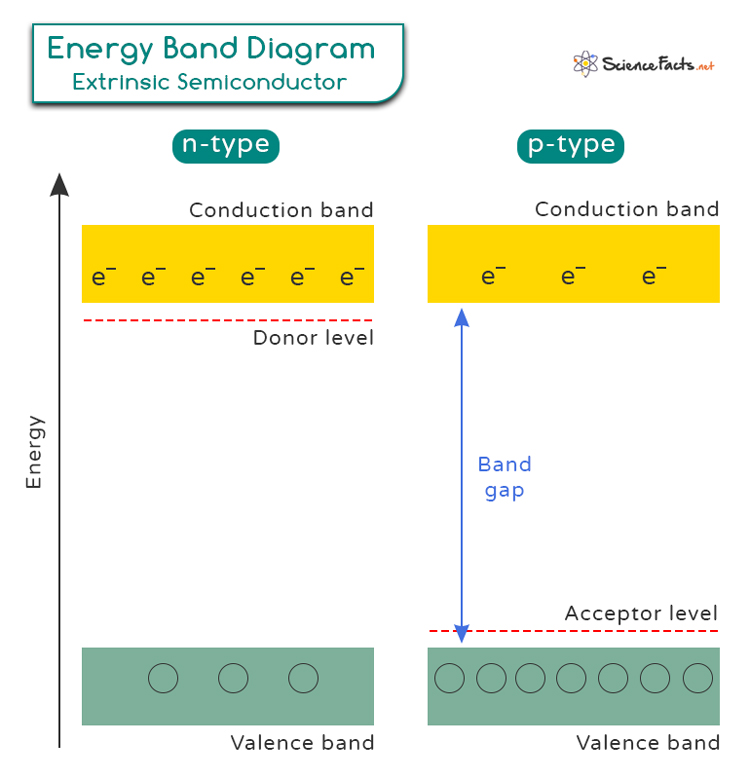
Extrinsic Semiconductor Band Diagram
Understanding the energy band diagrams of N-type and P-type semiconductors, we can see how doping affects the movement of charge carriers and enhances the electrical properties of the material. An energy band diagram consists of the following:
- Valence Band: The lower energy band filled with electrons.
- Conduction Band: The higher energy band where electrons can move freely, contributing to electrical conductivity.
- Band Gap: The energy gap between the valence band and the conduction band. Electrons need energy to jump from the valence band to the conduction band.
Depending on the type, the extrinsic semiconductor energy band diagram consists of two more levels in addition to the conduction and valence bands.
For an N-type semiconductor, the extra electrons from the dopant atoms form a new energy level just below the conduction band, called the donor level. At room temperature, it takes very little energy for these electrons to move from the donor levels to the conduction band, making them free to conduct electricity.
For a P-type semiconductor, the missing electrons create a new energy level just above the valence band. This level is called the acceptor level. When electrons from the valence band jump to the acceptor levels, they leave behind holes in the valence band, which can move and carry positive charges.
The energy band diagram below illustrates an N-type and a P-type semiconductor.
Uses and Applications
- Transistors: They typically combine N-type and P-type materials in configurations like NPN or PNP.
- Diodes: They are made by joining an N-type semiconductor and a P-type semiconductor, forming a PN junction diode.
- Integrated Circuits (ICs): They are fabricated using layers of N-type and P-type semiconductors to create complex circuits on a single chip.
- Solar Cells: They are typically made from silicon doped with different elements to create N-type and P-type layers.
- Sensors: They use properties of N-type and P-type materials to sense changes in light, temperature, pressure, etc.
Intrinsic vs. Extrinsic Semiconductors
| Characteristic | Intrinsic Semiconductor | Extrinsic Semiconductor |
|---|---|---|
| Origin | Pure semiconductor material | Semiconductor material with intentionally added impurities |
| Carrier Type | Electrons and holes (intrinsic carriers) | Electrons (N-type) or holes (P-type) as predominant charge carriers |
| Carrier concentration | An equal number of electrons and holes | Predominance of either electrons (N-type) or holes (P-type) depending on the dopant used |
| Dopants | No intentional dopants | Intentional addition of dopants to modify electrical properties |
| Conductivity | Relatively lower conductivity | Enhanced conductivity due to added charge carriers |
| Examples | Pure silicon or germanium | Silicon doped with phosphorus (N-type) or boron (P-type) |
| Applications | Used in essential electronic components like diodes and transistors | Widely employed in advanced electronic devices and integrated circuits |
-
References
Article was last reviewed on Tuesday, July 9, 2024
Related articles


Join our Newsletter
Fill your E-mail Address