Field-Effect Transistor
A Field-Effect Transistor, or FET, is a type of transistor that controls current flow through a semiconductor channel using an electric field. It is like a regular switch that controls electricity. FET is a voltage-controlled device. By applying voltage to one part, one can control how much current flows through another part. A FET is called a unipolar transistor because only electrons or holes operate as charge carriers.
How Does a FET Work
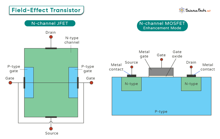
To understand how a FET works, let us look at its three main components: source, drain, and gate. They are connected to three terminals named accordingly. In addition, the channel is the region where current flows from the source to the drain. It is the conductive path formed between these two terminals when the transistor is turned on.
The key to the FET’s operation is the gate terminal, which is insulated from the channel by a thin layer of oxide. Applying a voltage to the gate creates an electric field that influences the channel’s conductivity. By varying this voltage, one can control the current, allowing for precise control within a circuit.
Types of FET
There are two types of FET: JFET (Junction Field-Effect Transistor) and MOSFET (Metal-Oxide-Semiconductor Field-Effect Transistor).
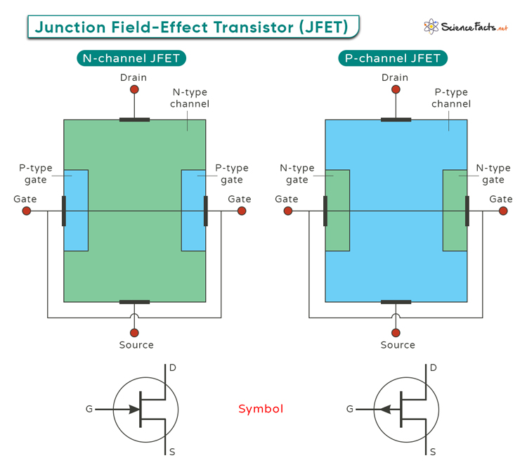
1. JFET
A JFET is characterized by a junction between the gate and the channel, offering simplicity and robustness. It comes in two forms: N-channel and P-channel.
- N-channel JFET: The channel is formed by electrons. A positive gate-to-source voltage enhances the channel conductivity by attracting electrons to the channel region, allowing current to flow.
- P-channel JFET: The channel is formed by hole. A negative gate-to-source voltage enhances the channel conductivity by attracting holes.
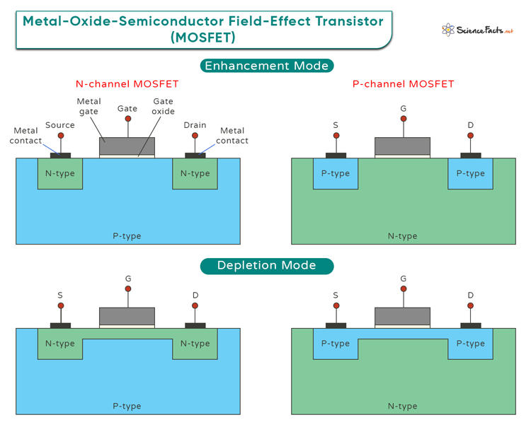
2. MOSFET
A MOSFET features a metal gate insulated by a thin oxide layer from the semiconductor. It has two operating modes: enhancement mode and depletion mode.
- Enhancement Mode: A voltage applied to the gate creates a conducting channel in the semiconductor, enabling current flow.
- Depletion Mode: The conducting channel exists by default, which diminishes as a voltage is applied to the gate.
These two modes give rise to four types of MOSFET.
- N-channel Depletion MOSFET
- P-channel Depletion MOSFET
- N-channel Enhancement MOSFET
- P-channel Enhancement MOSFET
Advantages
FETs are widely used in various electronic devices due to their high input impedance and low power consumption.
High Input Impedance: It helps reduce loading effects on preceding stages in a circuit, ensuring signal integrity and fidelity. This feature makes FETs suitable for applications where signal amplification and impedance matching are crucial.
Low Power Consumption: Its ability to operate at lower power levels without compromising performance makes it highly desirable in modern electronic design, especially portable electronic devices.
BJT vs. FET
Another commonly used type of transistor is the bipolar junction transistor (BJT). The table below captures the key differences between the two types.
| Characteristic | FET | BJT |
|---|---|---|
| Full form | Field Effect Transistor | Bipolar Junction Transistor |
| Control technology | Voltage-controlled | Current-controlled |
| Terminals | Source, Gate, Drain | Emitter, Base, Collector |
| Charge carriers | Majority carriers (electrons or holes) | Both majority and minority carriers (electrons and holes) |
| Device types | JFET (Junction FET), MOSFET (Metal-Oxide-Semiconductor FET) | NPN transistor, PNP transistor |
| Input impedance | High | Low |
| Switching speed | Generally higher than BJT | Generally lower than FET |
-
References
Article was last reviewed on Tuesday, June 10, 2025
Related articles


Join our Newsletter
Fill your E-mail Address