PN Junction
The PN junction is a key concept in semiconductor physics and is the foundation for many electronic devices, such as smartphones and computers. It is formed when two types of extrinsic semiconductor, P-type and N-type, are brought into contact. The P-type semiconductor contains excess positively charged carriers or holes, while the N-type semiconductor contains excess negatively charged carriers or electrons. The importance of a PN junction lies in its ability to regulate the flow of electrical current, a feature exploited in various electronic applications like rectifiers in power supplies and LEDs in electronic devices.
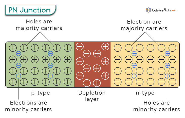
Depletion Region
When a P-type and an N-type semiconductor are joined, the region where they meet is called the depletion region. In this region, free charge carriers (electrons and holes) have diffused away, leaving behind charged ions. The depletion region is a barrier, preventing further movement of free charge carriers across the junction. It is like a boundary region where positive and negative charges are fixed and cannot move, creating an electric field that blocks current flow unless an external voltage is applied.
We can draw an analogy based on the behavior of charge carriers. Imagine a wall and people attempting to cross it. The barrier is similar to the wall, and the free charge carriers are like people.
Biasing of PN Junction
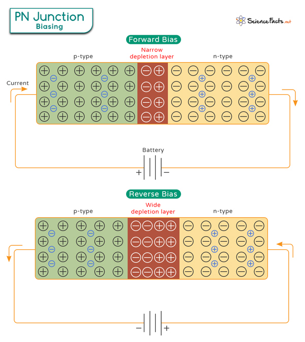
Biasing refers to the process of applying an external voltage across a PN junction that alters the depletion region’s characteristics. There are two main types of biasing: forward bias and reverse bias.
Forward Bias
Forward bias refers to the situation where the positive terminal of a battery connects to the P-type region, and the negative terminal connects to the N-type region of a PN junction. As a result, the barrier across the PN junction is reduced, diminishing the resistance and allowing for a more effortless flow of charge carriers across both regions.
Electrons from the N-type semiconductor move toward the P-type semiconductor, and holes from the P-type semiconductor move toward the N-type semiconductor. This is like lowering the height of our imaginary wall, making it easier for people to cross. This movement of charge carriers constitutes an electric current in a diode, a simple semiconductor device based on a PN junction.
Reverse Bias
During reverse bias, the positive terminal of the battery is connected to the N-type semiconductor, and the negative terminal is connected to the P-type semiconductor. The external voltage enhances the barrier that naturally exists at the junction in an unbiased state, making it very hard for charge carriers to cross. Again, we can bring the wall analogy. Increasing the height of the wall makes it difficult for people to cross. Because of the high resistance, the current is limited to a minimum value in the diode.
I-V Characteristics of a PN Junction Diode
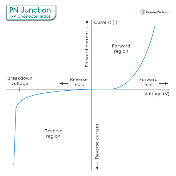
The I-V curve shows how the current through a diode changes with different voltages and helps us understand how it behaves in circuits. The graph typically shows the relationship between the forward and reverse bias voltage applied across the diode and the resulting current flowing through it.
Equilibrium State
The equilibrium state is the condition when a depletion region forms in the diode. In this state, there is minimal current flow across the junction as the diffusion of carriers is balanced by the built-in potential.
Forward Bias Behavior
When the diode is forward-biased, the barrier is lowered. At first, a small current starts to flow. As the voltage increases, a lot more current flows because more charge carriers help conduct the electricity. In this state, the diode has low resistance and lets much current pass through.
Reverse Bias Behavior
Reverse bias increases the barrier, preventing the majority charge carriers from easily crossing the junction and resulting in minimal current flow. This tiny current is known as reverse leakage current. It occurs because minority carriers (holes from the N-region and electrons from the P-region) still move across the junction. This leakage current can be considered negligible compared to the forward bias condition. The reverse-biased PN junction exhibits high electrical resistance, and the diode is an insulator to the applied voltage until the voltage reaches a limit.
Breakdown
When the reverse voltage on the diode becomes too high, the current suddenly increases, causing the diode to lose its ability to block current. This phenomenon is called breakdown, and the voltage at which it happens is called the breakdown voltage. Learn more about breakdown in Zener diode.
Applications of PN Junction Diode
- As a rectifier, which converts Alternating Current to Direct Current
- As a Zener diode that is used in circuits for voltage regulation
- As a fundamental building block for the construction and operation of PNP transistor and NPN transistor, which contain multiple PN junctions.
- As switches in electrical circuits that turn smaller circuits on and off within more complex systems. This feature comes from the fact that diodes only allow current to pass in the forward bias direction.
- As a photodiode during a reverse bias operation because it is sensitive to light
- As an LED, which emits light when in forward bias
-
References
Article was last reviewed on Tuesday, July 9, 2024
Related articles


Join our Newsletter
Fill your E-mail Address