Intrinsic Semiconductor
Intrinsic semiconductors are pure semiconductor materials that are made from a single element or compound with no added impurities or atoms. These materials typically consist of elements from Group IV of the periodic table, such as silicon or germanium.
Their electrical conductivity is determined by the temperature and the inherent properties of the material itself. Unlike extrinsic semiconductors, which are doped with impurities to alter their electrical properties, intrinsic semiconductors do not have intentional impurities added.
Charge Carriers in Intrinsic Semiconductors
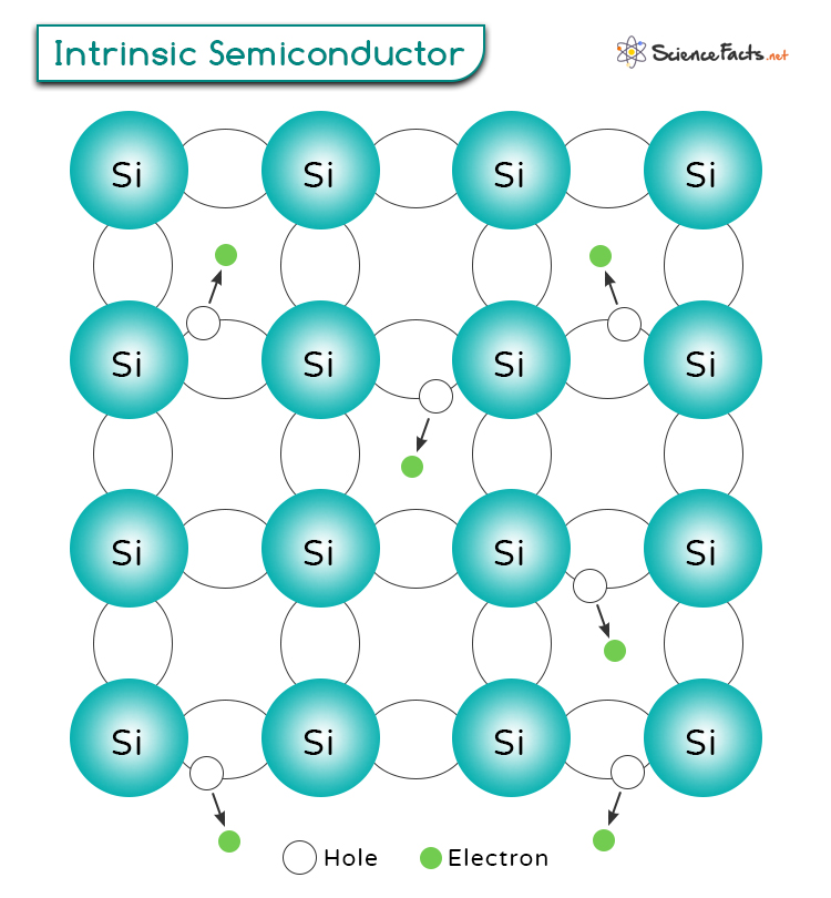
Charge carriers are particles that carry electric charge and enable the flow of electrical current in a material. In semiconductors, the main charge carriers are electrons, which have a negative charge, and “holes”, which lack an electron and can be thought of as positive charges. While they do not represent real particles like electrons, holes facilitate current flow by behaving like positive charge carriers.
Movement of Charge Carriers
The movement of charge carriers, specifically electrons, is crucial in determining the current flow within a semiconductor. In an intrinsic semiconductor, some electrons gain enough energy to break free from their atomic bonds through various mechanisms such as applied electric field, thermal excitation, and exposure to light. These free electrons become mobile and contribute to the conductivity of the material.
Carrier Concentration

For an intrinsic semiconductor, the concentration of electrons in the conduction band is equal to the concentration of holes in the valence band. Suppose ne is the intrinsic electron concentration, and nh is the intrinsic hole concentration. Then,
ne = nh = ni
Where ni is the intrinsic carrier concentration, which refers to either the intrinsic electron or hole concentration.
The table below shows the intrinsic carrier concentrations of a few semiconductors at room temperature. The free electron density of copper, which is a pure conductor, is also shown for comparison.
| Material | Intrinsic Carrier Concentration at 300 K (cm-3) |
|---|---|
| Si | 1.0 x 10¹⁰ |
| Ge | 2.0 x 10¹³ |
| GaAs | 2.0 x 10⁶ |
| Cu | 8.47 x 10²² |
Electrical Conduction in Intrinsic Semiconductors
Absolute Zero
Absolute zero is the lowest possible temperature at which a material has no thermal energy. At this temperature, all electrons in an intrinsic semiconductor are tightly bound to their atoms, so there are no free electrons or holes. Therefore, the material behaves like an insulator, meaning it does not conduct electricity.
Higher Temperature
When the temperature rises, the material gains thermal energy. This energy can excite electrons, giving them enough energy to break free from their atoms. When an electron breaks free, it moves to the conduction band, where it can flow and conduct electricity. The absence of the electron in the atom creates a hole in the valence band, resulting in an equal number of electrons and holes.
So far, we have seen the random movement of electrons and holes due to thermal energy. Let us examine what happens when an electric field is applied.
Presence of Electric Field
When an electric field is applied across a semiconductor material, it exerts a force on the charge carriers, thereby influencing their movement. Free electrons in the conduction band experience a force in a direction opposite to that of the electric field. These electrons move toward the positive terminal of the applied voltage.
Holes in the valence band experience a force in the same direction as the electric field. As electrons from neighboring atoms move to fill these holes, they effectively move toward the negative terminal of the applied voltage, causing the holes to appear to move in the opposite direction.
This collective motion constitutes an electric current within the semiconductor. In intrinsic semiconductors, the ability to conduct electricity depends on the number of charge carriers.

Uses and Applications
- Thermistors: The resistance of intrinsic semiconductors changes significantly with temperature, making them useful for precise temperature measurements in devices that measure temperature, such as thermistors.
- Radiation Detectors: When radiation interacts with intrinsic semiconductors, it generates electron-hole pairs, leading to a measurable current. This property is useful in medical imaging, environmental monitoring, and nuclear physics research.
- Photodetectors: When light hits an intrinsic semiconductor, it generates electron-hole pairs, creating a current that can be measured. Devices that convert light into electrical signals are called photodetectors.
- Fabrication of Doped Semiconductors: Intrinsic semiconductors are used as the starting material for creating doped semiconductors. Doping involves adding small amounts of impurities to an intrinsic semiconductor to change its electrical properties, which is essential for creating components like diodes, transistors, and integrated circuits.
-
References
Article was last reviewed on Tuesday, July 23, 2024
Related articles


Join our Newsletter
Fill your E-mail Address