Semiconductor
Semiconductors are materials with unique properties that allow them to conduct electricity under certain conditions. Their electrical conductivity lies between conductors, which conduct electricity easily, and insulators, which block electrical flow. This unique property makes them essential components in electronic devices and applications.
Examples of semiconductors include silicon (Si), germanium (Ge), gallium arsenide (GaAs), gallium nitride (GaN), indium phosphide (InP), and silicon carbide (SiC).
Properties of Semiconductors
- Electrical Conductivity: Semiconductors have electrical conductivity between that of conductors, like copper and aluminum, and insulators, like glass and diamond. Conductivity in semiconductor materials is influenced by temperature, impurity concentration, and applied voltage.
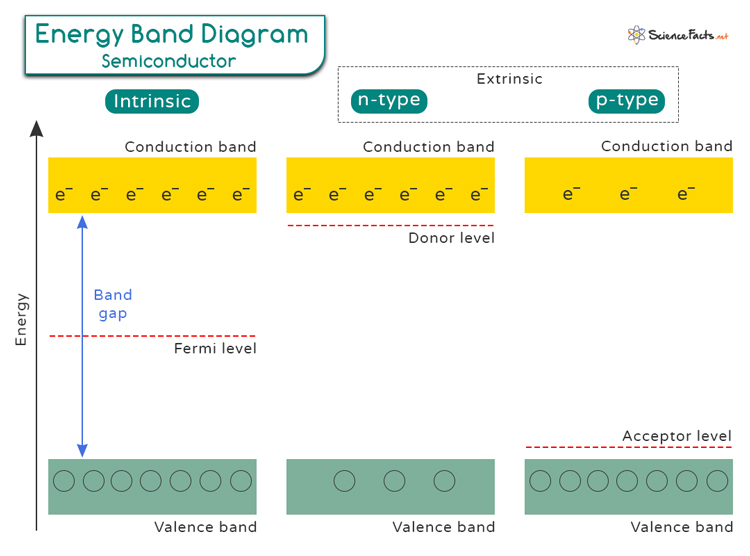
- Energy Band Gap: Semiconductors have a well-defined energy band gap between the valence band, where electrons are bound to atoms, and the conduction band, where electrons can move freely. This gap determines how easily electrons can be excited to conduct electricity.
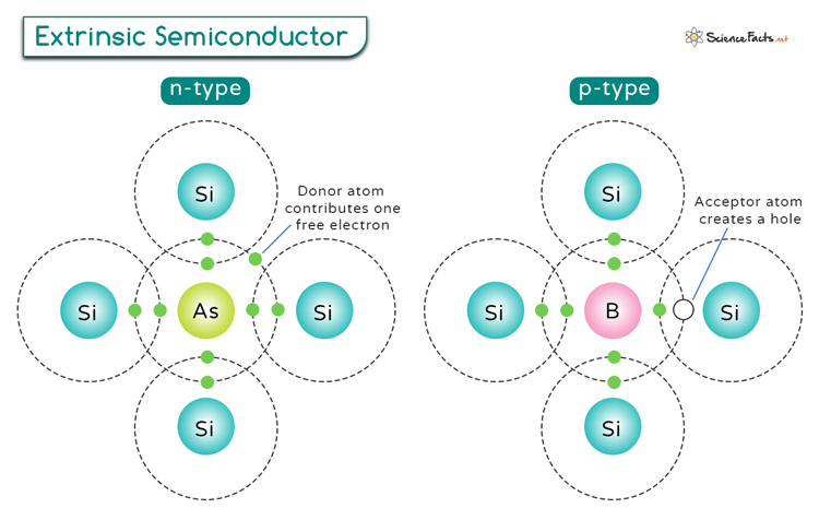
- Doping: Adding impurities (trivalent or pentavalent atoms) to a semiconductor can change its electrical properties. N-type doping introduces more free electrons, while P-type doping creates more “holes”, which are positive charge carriers.
- Temperature Sensitivity: The conductivity of semiconductors increases with temperature, unlike conductors. This is because more electrons gain enough energy to jump from the valence band to the conduction band.
- Photoconductivity: When exposed to light, semiconductors conduct electricity better. This property is utilized in devices like solar cells and light sensors.
- Thermal Conductivity: Semiconductors generally have lower thermal conductivity compared to metals, meaning they do not conduct heat as well.
- Optical Properties: Semiconductors can absorb and emit light, making them essential for LEDs and laser diodes.
- Carrier Mobility: This refers to how quickly electrons or holes can move through the semiconductor material. The charge carrier mobility depends upon the impurity concentration, temperature, and applied electric field.
Carrier Mobility in Semiconductor
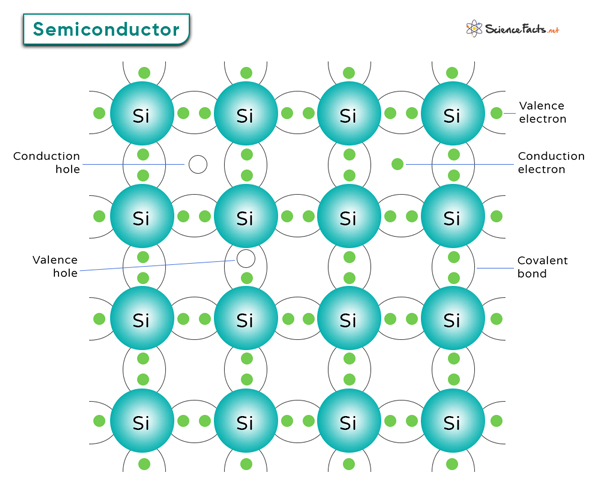
In a semiconductor, carriers refer to the particles that carry electric charge and enable the flow of electricity through the material. There are two types of carriers.
1. Electrons: These are negatively charged carriers that can move through the semiconductor material, contributing to electric current. Electron mobility refers to how easily electrons can move through a semiconductor material when subjected to an electric field. The higher the electron mobility, the faster the electronic device with better performance.
2. Holes: These are the absence of an electron in the valence band, effectively acting as positively charged carriers. When an electron leaves its position in the valence band, it leaves behind a hole that can move as neighboring electrons jump to fill it. Hole mobility represents the movement of holes within a semiconductor lattice.
The behavior of charge carriers within semiconductors is essential for optimizing their performance. To understand how charge carriers are created and responsible for conducting electricity, let us delve into semiconductor band theory.
Band Theory of Semiconductors
Band theory in semiconductors explains how electrons are arranged in energy bands. The valence band contains electrons tightly bound to atoms, while the conduction band holds electrons that can move freely. The energy gap between these bands is called the band gap, which is denoted in the unit of electron volts (eV). Below is a table that shows the energy band gap values of different semiconductors at 300 K.
| Semiconductor | Energy Band Gap (eV) at 300 K |
|---|---|
| Silicon (Si) | 1.11 |
| Germanium (Ge) | 0.66 |
| Galium Arsenide (GaAs) | 1.43 |
| Indium Phosphide (InP) | 1.27 |
| Gallium Phosphide (GaP) | 2.25 |
When thermally excited, electrons can jump from the valence band to the conduction band, creating electron-hole pairs. These charge carriers are responsible for electrical conductivity in semiconductors.
Types of Semiconductor
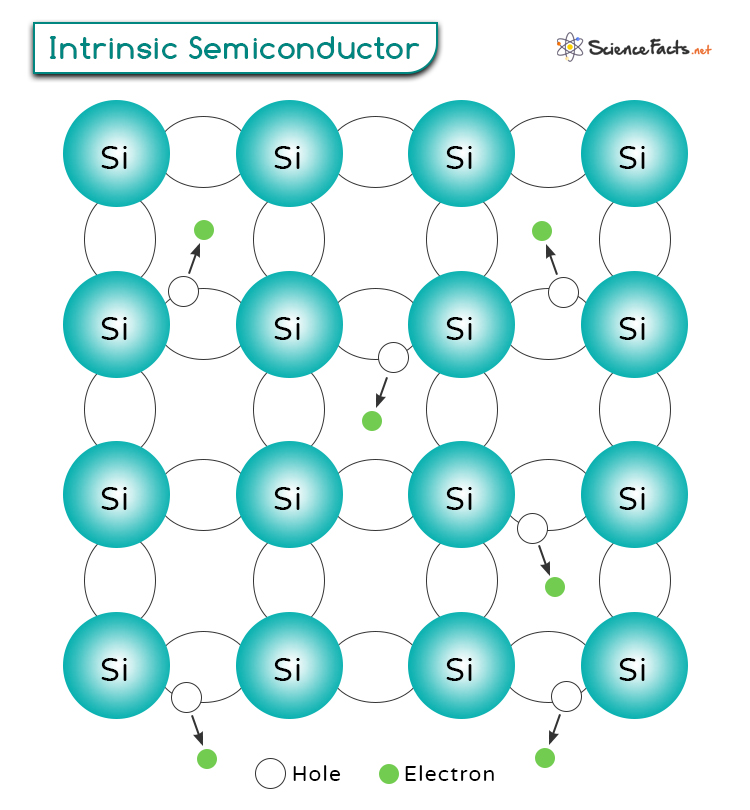
Intrinsic Semiconductors: They are pure semiconducting materials like silicon or germanium. Their electrical properties are determined by their structure. They have a limited number of charge carriers that can be easily excited by heat or electric field to conduct electricity.
Extrinsic Semiconductors: They are doped with impurities to enhance their conductivity. By adding specific atoms like phosphorus or boron to the crystal lattice of the semiconductor material, engineers can increase the number of charge carriers and modify its electrical properties. The next section discusses doping in extrinsic semiconductors.
This interplay between intrinsic properties and extrinsic modifications allows precise control over semiconductor behavior.
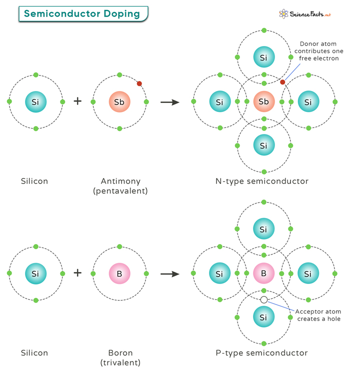
Doping in Semiconductors
Doping is a crucial process in semiconductor technology that involves introducing impurities into a pure semiconductor material to alter its electrical properties. There are two main types of doping: N-type and P-type, each with distinct effects on the semiconductor’s conductivity.
N-type: This doping type involves adding elements such as phosphorus or arsenic to a semiconductor material like silicon. These elements have one extra electron compared to silicon atoms, making them donors of electrons. When these donor atoms are introduced into the semiconductor crystal lattice, they release free electrons into the material, increasing its electron concentration. This excess of negatively charged electrons gives rise to an N-type semiconductor with high electron conductivity.
P-type: This doping type involves adding elements like boron or gallium to silicon. These elements have one less electron than silicon atoms, creating “holes” in the crystal lattice where an electron is missing. These “acceptor” atoms attract nearby electrons, creating spaces for new electrons to move in – effectively creating positively charged holes that behave as charge carriers. This results in a P-type semiconductor with increased hole concentration and enhanced hole conductivity.
Applications of Semiconductor
- Computers and Smartphones: Semiconductors are used in microprocessors and memory chips, which are the brains of computers and smartphones, enabling them to process information and store data efficiently.
- Solar Panels: Solar panels’ photovoltaic cells are made from semiconductor materials like silicon. They convert sunlight into electricity, providing a renewable energy source.
- LEDs and Displays: Light-emitting diodes (LEDs) and display screens use semiconductors to produce light and vibrant colors in devices such as TVs, monitors, and digital billboards.
- Medical Devices: Semiconductors are essential in medical equipment like MRI machines, ultrasound devices, and portable diagnostic tools, enhancing medical imaging and patient monitoring.
- Automobiles: Modern cars rely on semiconductor chips for various functions, including engine control units, navigation systems, and advanced driver-assistance systems (ADAS), improving safety and efficiency.
- Communication Systems: Semiconductors are critical in wireless communication devices, such as smartphones, routers, and satellites, enabling high-speed data transmission and connectivity.
- Consumer Electronics: Everyday gadgets like digital cameras, gaming consoles, and household appliances use semiconductor components to function, making our lives more convenient and entertaining.
- Industrial Automation: Semiconductors power sensors, controllers, and robotics in industrial automation, increasing productivity and precision in manufacturing processes.
-
References
Article was last reviewed on Friday, August 8, 2025
Related articles


One thought on “Semiconductor”
Leave a comment


Join our Newsletter
Fill your E-mail Address
I LIKE YOUR NOTE THANKS!!!