NPN Transistor
An NPN transistor is a type of bipolar junction transistor (BJT), which is a semiconductor device used to amplify or switch electronic signals.
Construction
The construction of an NPN transistor involves carefully doping three different semiconductor layers (silicon or germanium) to create the desired behavior.
Components
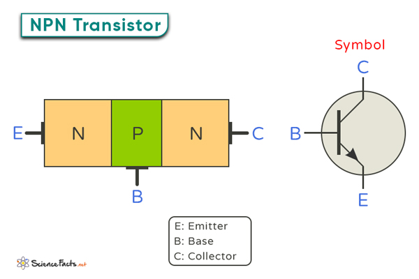
A thin P-type semiconductor layer is sandwiched between two thicker N-type semiconductor layers, which are referred to as the emitter (E), base (B), and collector (C).
Emitter: It is heavily doped with excess electrons, allowing for efficient injection of charge carriers into the base region.
Base: It is lightly doped and narrow compared to the emitter. It facilitates the diffusion of charge carriers injected from the emitter to the collector.
Collector: It is moderately doped. Its primary function is to collect the electrons emitted by the emitter and pass through the base.
Junctions
Two junctions are formed within the transistor structure:
Emitter-base (EB) junction: It is formed between the emitter and the base.
Collector-base (CB) junction: It is formed between the collector and the base.
Working Principles
Biasing
To make the NPN transistor work normally, biasing must be applied to its junctions.
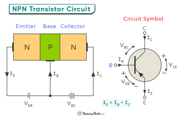
The emitter-base junction is forward-biased, meaning the N-type emitter is connected to the negative terminal of the supply voltage (VBE), while the P-type base is connected to the positive terminal.
The collector-base junction is reversed-biased, meaning the N-type collector is connected to the positive terminal of the supply voltage (VBC), while the P-type base is connected to the negative terminal. The reverse biasing of the CB junction creates a wider depletion region than the EB junction, preventing electrons from flowing from the base into the collector.
Current Flow
In an N-type emitter, electrons are the predominant charge carriers. They initiate their flow from the emitter to the P-type base, resulting in current. This current flows across the emitter-base junction called the emitter current (IE).
These electrons proceed into the base region, where holes are the predominant charge carriers. However, due to its thinness and light doping, a few holes are available for recombination with the electrons. While most electrons traverse the base region, only a fraction recombines with the available holes. As a result of this recombination process, a current flows through the circuit, denoted as the base current (IB). This base current is notably smaller than the emitter current (IE).
Most electrons continue through the depletion region of the collector-base junction and into the collector region. The resultant current flow carried by these remaining electrons is the collector current (IC) and is substantially larger than the base current.
The relationship between IE, IB, and IC is as follows:
IE = IB + IC
Regions of Operation
An NPN transistor operates in three distinct regions, each corresponding to different biasing conditions of the junctions.
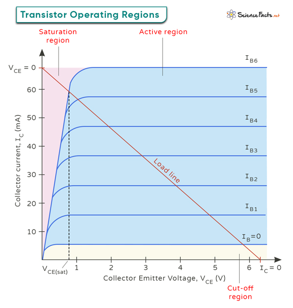
1. Cut-off Region
In the cut-off region, both the emitter-base and collector-base junctions are reverse-biased. The transistor acts as an open switch, meaning no significant current flows between the collector and emitter terminals. It occurs when the voltage applied to the base terminal is below a certain threshold, which is insufficient to allow the transistor to conduct. This state is an ideal choice for applications where precise control over current flow is necessary, such as in digital logic circuits.
2. Active Region
In the active region, the emitter-base junction is forward-biased, and the collector-base junction is reverse-biased. The transistor operates as an amplifier, and the collector current is proportional to the base current. This characteristic is used in analog circuits for amplification.
3. Saturation Region
In the saturation region, both the emitter-base and collector-base junctions are forward-biased. The transistor behaves as a closed switch, allowing maximum current to flow between the collector and emitter terminals. This state is achieved when the voltage applied to the base terminal is sufficiently high, enabling the transistor to conduct fully. Saturation mode is crucial in applications requiring the transistor to carry a significant amount of current, such as in power control circuits or motor drivers.
-
References
Article was last reviewed on Monday, July 8, 2024
Related articles


Join our Newsletter
Fill your E-mail Address