Bipolar Junction Transistor
A bipolar junction transistor (BJT) is a three-layered device that helps conduct the flow of electricity. It consists of both types of extrinsic semiconductor: P-type and N-type. A BJT can be compared to a sandwich with three layers of doped semiconductors (which come from semiconductor doping). These layers are called the emitter, base, and collector. The BJT works based on the movement of charge carriers, like electrons and holes, between the layers.
Types of BJT
There are two types of BJT, each with its characteristics and uses.
- NPN Transistor: A thin layer of P-type semiconductor sandwiched between two thick N-type semiconductor layers. Here, electrons serve as the majority charge carriers.
- PNP Transistor: It has two layers of P-type semiconductors sandwiching an N-type layer, an arrangement opposite to the NPN transistor. The majority charge carriers are holes.
The two types and their symbols are shown in the image below.
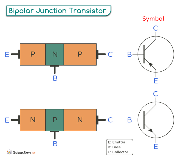
Structure of BJT
The emitter, base, and collector are carefully doped to achieve specific electrical characteristics.
Emitter
The emitter is heavily doped with excess electrons or holes. This heavy doping allows for efficient injection or emission of charge carriers into the base region.
Base
The base is adjacent to the emitter and is lightly doped compared to the former. It is usually very narrow to facilitate the diffusion of charge carriers injected from the emitter to the collector. The base controls how many charge carriers reach the collector. Together with the emitter, the base forms the emitter-base junction.
Collector
The collector, located opposite the emitter, is moderately doped. Its primary function is to collect the majority charge carriers emitted by the emitter and pass through the base. The collector and the base together form a junction known as the collector-base junction. During normal operation, this junction is reverse-biased, allowing the collector to collect charge carriers that diffuse across the thin base region.
The physical structure of a BJT often involves sandwiching the lightly doped base between the heavily doped emitter and the moderately doped collector. This configuration enables the transistor to amplify and control the current flow between the emitter and the collector. A small current entering the base can control a much larger current flowing from the emitter to the collector. The precise doping levels and physical dimensions of these layers determine the transistor’s characteristics and functionality in electronic circuits.
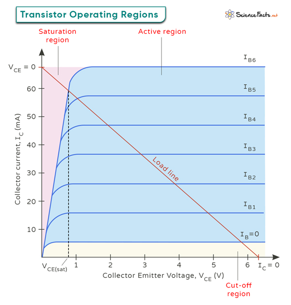
Regions of Operation in BJT
1. Cut-off Region
In this region, the transistor is turned off. The base-emitter and base-collector junctions are reverse-biased, resulting in minimal or zero current flow. The transistor is effectively turned off, and no amplification or switching occurs.
2. Active Region
Also known as the amplification region, this region is where the transistor amplifies signals. For the BJT to operate in the active region, the base-emitter junction must be forward-biased, and the base-collector junction must be reverse-biased. It allows a controlled amount of current to flow through the transistor. In this region, small changes in input signals can result in significant output variations, making it ideal for amplification.
3. Saturation Region
In this region, the transistor acts like a closed switch. Both the base-emitter and base-collector junctions are forward-biased, allowing maximum current to flow through the transistor. The current flowing from the collector to the emitter is at its maximum and does not depend on the base current anymore. This region is useful for switching applications, where the transistor turns circuits on and off.
BJT Configuration
1. Common Base (CB)
The input and output circuits share the base terminal. The input signal is applied between the emitter and the base, while the output is taken across the collector and the base. The base terminal is usually grounded or connected to a reference point.
For the transistor to function in this setup, the current entering the emitter must be greater than the base and collector currents. As a result, the collector current output is less than the emitter current input, resulting in a current gain of one or less.
2. Common Emitter (CE)
In this configuration, the emitter is grounded and common to both the base and the collector. The input signal is applied between the base and the emitter, while the output is taken from between the collector and the emitter.
This configuration offers several advantages, including high voltage gain, a good input-output phase relationship, and relatively low output impedance. These features make it useful in many electronic circuits.
3. Common Collector (CC)
This configuration is known as a Voltage Follower or Emitter Follower circuit. The collector terminal is common to the input and output circuits. The input signal is applied between the base and the collector, and the output is taken from the emitter and the collector.
This configuration offers a high input impedance and a low output impedance, making it an excellent choice for impedance matching and voltage buffering. It provides a voltage gain of one (meaning the output voltage is the same as the input voltage) but offers a significant current gain.
The following table illustrates the characteristics of the various BJT configurations:
| Characteristics | Common Base | Common Emitter | Common Collector |
|---|---|---|---|
| Power Gain | Low | Very high | Medium |
| Current Gain | Low | Medium | High |
| Voltage Gain | High | Medium | Low |
| Power Gain | Low | Very high | Medium |
| Input Impedance | Low | Medium | High |
| Output Impedance | Very high | High | Low |
| Phase Angle | 0° | 180° | 0° |
-
References
Article was last reviewed on Friday, July 12, 2024
Related articles


Join our Newsletter
Fill your E-mail Address