Schottky Diode
A Schottky diode is an electronic device that allows electricity to flow in one direction with very little resistance and can switch on and off very quickly. It features a small rectifying junction, which differs from a traditional PN junction. This special design means it does not have a depletion layer, which helps it respond faster and use less power, making it essential in many modern electronics.
The Schottky diode is named after Walter H. Schottky, a German physicist who contributed to its development.
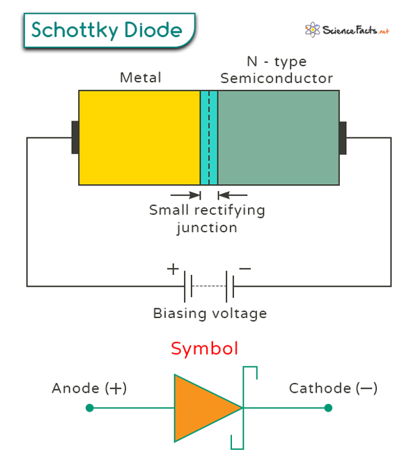
Structure and Symbol
The small rectifying junction is formed between a metal, such as platinum, gold, or aluminum, and an N-type semiconductor (typically silicon). The metal forms the anode, while the N-type semiconductor forms the cathode.
The symbol used to represent a Schottky diode in circuit diagrams is similar to that of a standard diode with a modified cathode to reflect its unique characteristics.
Working Principle
The working principle of a Schottky diode revolves around its unique metal-semiconductor junction, which leads to distinctive properties compared to a traditional PN junction diode.
Barrier Formation
When a metal, such as platinum or gold, comes into contact with a semiconductor material like silicon or gallium arsenide, it forms a potential energy barrier due to differences in their work functions. Work function is the energy required for electrons to escape. This barrier, called Schottky barrier, prevents the majority carriers (electrons) from readily moving across the junction. It differs from a PN diode in that it is not formed by the diffusion of charge carriers.
Conductivity and Current Flow
The rectifying metal-semiconductor junction can be described by the current flow under forward and reverse biasing.
Forward Bias: When a forward voltage is applied across the diode, i.e., positive on the metal side, electrons (majority carriers) from the semiconductor material overcome the potential barrier and flow into the metal. This allows current to flow easily, making the diode highly conductive.
Reverse Bias: When a reverse voltage is applied, i.e., positive on the semiconductor side, the barrier prevents the electrons from crossing. This results in minimal current flow.
I-V Characteristics
The I-V characteristics of a Schottky diode provide crucial insights into its behavior regarding current flow under varying voltage conditions. Due to its metal-semiconductor junction construction, the relationship between the current and voltage across the diode primarily exhibits distinct non-linear behavior, similar to the exponential curve of a PN junction diode.
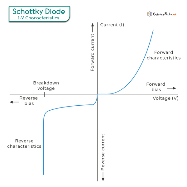
Forward Bias Behavior: Low Forward Voltage Drop
Schottky diodes need very little voltage to start conducting electricity. Its knee voltage is 0.3 to 0.4 volts. Even a small increase in voltage results in a large increase in current. This behavior arises from the absence of a depletion region, leading to a quick injection of electrons across the metal-semiconductor interface.
Reverse Bias Behavior: Minimal Leakage Current
When a reverse voltage is applied, only a small amount of current leaks through. This happens because there are fewer minority carriers and electrons quickly recombine with them near the metal-semiconductor interface. However, Schottky diodes typically exhibit a higher reverse leakage current than conventional PN junction diodes due to the absence of the depletion layer, making them less suitable for applications requiring stringent reverse bias requirements.
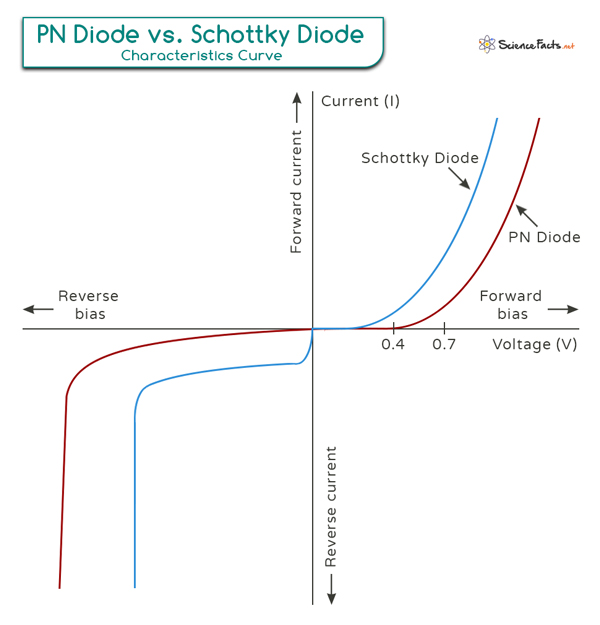
PN Diode vs. Schottky Diode
The image below compares the characteristics curves of Schottky and PN diodes. While both diodes exhibit non-linear current-voltage characteristics, the Schottky diode tends to have lower forward voltage drop and faster response but higher reverse leakage voltage than the PN junction diode.
Advantages and Disadvantages
Advantages
- Lower forward voltage drop (0.15 to 0.45 volts) than a PN junction diode (0.7 volts) means that it wastes less energy as heat. This feature is efficient in low-voltage applications like power supplies and power converters.
- Fast switching capability makes it essential for high-speed and high-frequency applications. It is crucial for radio frequency and microwave circuits, which are used in communication devices and radar systems.
- Combination of low forward voltage drop and fast switching results in high overall efficiency.
- Fast response helps protect clamping circuits from transient voltage spikes and over-voltage conditions. It enhances the reliability and longevity of electronic devices like smartphones, tablets, and computers.
- Can be made smaller than a traditional diode while maintaining its performance characteristics. This characteristic benefits modern electronic devices like smartphones, wristwatches, and solar cells.
Limitations
- Higher reverse leakage currents than silicon PN-junction diodes can be a drawback in certain applications.
- Lower reverse voltage rating makes them unsuitable for high-voltage applications.
-
References
Article was last reviewed on Tuesday, July 23, 2024
Related articles


Join our Newsletter
Fill your E-mail Address