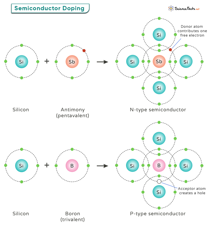
Semiconductor Doping
Semiconductor doping is a key process in electronics. It involves adding tiny amounts of specific impurities to a pure semiconductor material, like silicon, to change its electrical properties. This process helps the semiconductor conduct electricity better and makes electronic devices like transistors and diodes work properly.
What Happens During Doping
By adding small amounts of specific impurities (dopants) to the semiconductor crystal, one can create regions with extra electrons (N-type) or regions with missing electrons, called “holes” (P-type). Thereby, doping allows engineers to control the electrical properties of semiconductor materials.
Creating a PN Junction
Doping is crucial for creating a PN junction, a key component in many semiconductor devices. When a P-type semiconductor comes into contact with an N-type semiconductor, they form a PN junction. This junction acts like a gate, controlling the flow of electrical current. It allows current to flow easily in one direction but not in the opposite direction, which is essential for devices like diodes used in rectifiers and voltage regulators.
Types of Semiconductor Doping
There are two main types of semiconductor doping: P-type and N-type. Together, they give rise to an extrinsic semiconductor.
1. P-type
In P-type doping, impurities create an excess of positively charged holes in the crystal lattice, changing its conductivity. Elements from Group III of the periodic table, like boron, aluminum, or gallium, are used. These elements have one less valence electron than the semiconductor, creating positively charged vacancies when they replace semiconductor atoms. These holes attract free electrons, contributing to the material’s conductivity.
2. N-type
N-type doping increases the number of mobile negative charge carriers. Group V elements like phosphorus, arsenic, and antimony are common N-type dopants. These elements have five valence electrons, one more than the four in an undoped semiconductor, resulting in an extra electron. Introducing these dopants into the semiconductor replaces some host atoms with dopant atoms. This creates excess electrons, which are free to move and enhance conductivity, defining N-type semiconductor material.
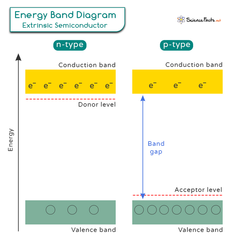
Effect of Doping on Energy Band Gap
Band theory is a fundamental concept in semiconductor physics that helps us understand how electrons are positioned in different materials. In a semiconductor material, the valence band is the highest energy band that is completely filled with electrons at absolute zero temperature. The conduction band, on the other hand, is the next higher energy band that remains empty at absolute zero.
When a semiconductor is doped with impurities, new energy levels are introduced within the band gap (the energy gap between the valence band and the conduction band). They are known as donor level in N-type and acceptor level in P-type. For P-type semiconductors, the impurities create holes in the valence band. Conversely, for N-type semiconductors, the impurities introduce extra electrons in the conduction band.
-
References
Article was last reviewed on Tuesday, June 10, 2025
Related articles


3 thoughts on “Semiconductor Doping”
Leave a comment

Join our Newsletter
Fill your E-mail Address
most authentic and to-the-point facts of science relevant to save me from stress and strain.
With China recently restricting their exports of antimony can we use more phosphorus for n doping of semiconductors? Any other element? This may be a critical problem.
Phosphorus and arsenic are other dopants.